Imagine a world without your mobile phone, computer, or digital camera. Without Jan Czochralski’s revolutionary discovery, that’s the world we’d be living in today. His eponymous Czochralski method is the foundation for producing 95% of the world’s microchips that underpin semiconductors and integrated circuits -the hearts and brains that run nearly all things tech, from laptops, autonomous cars, and spaceships to solar cells, AI, VR, and quantum computing.
As Srabanti Chowdhury, a professor of electrical engineering at Stanford University, says, Jan Czochralski was, “without question, one of the most consequential scientific minds in history.”
Pat Gelsinger, former CEO and CTO of Intel, agrees, emphasizing that “His elegant crystallization process remains the foundation upon which so much of our world stands.
”Czochralski’s discovery is the backbone of modern electronics, enabling our connected world, communications, transportation, healthcare, commerce, and society to function.
Beyond digital technology, the Czochralski method also sparked a booming, multi-billion-dollar industry in flawless, lab-made jewels — synthetic crystals like diamonds, sapphires, and emeralds.
What is the Czochralski Method?
The Czochralski method is a pivotal crystal-growing technique that underpins our modern digital age. It was discovered by Jan Czochralski in 1916 through a remarkable accident. While working in his lab, he mistakenly dipped his quill pen into a well of molten tin instead of ink. Upon pulling it out, Czochralski observed a long metal thread and realized he had produced a single crystal.
This seemingly simple discovery proved to be a game-changer. While Czochralski didn't patent the method at the time because he couldn't foresee a direct application, its value later became immeasurable. Scientists and engineers refined his process, which became essential for producing the ultrapure silicon wafers used in microchips.
In 1958, five years after Czochralski’s death, scientists at Bell Labs and Texas Instruments began applying the method to create integrated circuits, laying the groundwork for the rise of computing technology. Today, the technique allows for the precise "growing" of perfect crystals from melted minerals, fundamentally transforming various industries.
Who was JanCZ?
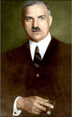
Jan Czochralski was an extraordinary individual – a self-taught genius and a true polymath, whose journey spanned humble beginnings to widespread recognition, and tragically, to profound obscurity.
“I have enough wealth, I have enough fame, my country Poland needs me now.”
Born in 1885 in Kcynia, Poland, he eschewed college to pursue his fascination with metallurgy. His life was a testament to perseverance and dedication to science. Beyond the Czochralski method, he achieved fame and wealth with "Metal B," a tin-free bearing alloy used in the railroad industry, and invented a radio microscope, a predecessor to modern scanning microscopes. He even dabbled in poetry, developed a recipe for shoe polish, and a remedy for colds. Henry Ford recognized his brilliance and invited him to the U.S., but Czochralski declined, stating, “I have enough wealth, I have enough fame, my country Poland needs me now.”
Czochralski’s life took a dramatic turn with the Nazi invasion of Poland, where he used his connections to aid Poles and Jews while working with the Polish resistance. But six years on, after WWII, he was falsely accused of collaboration with the Germans by the Soviet communists, resulting in the destruction of his academic career, seizure of his possessions, and his banishment to his childhood hometown. He died in obscurity in 1953, all but penniless.
For decades, Czochralski’s legacy was suppressed. It wasn't until the early 2000s that Polish scientist Dr. Pawel Tomaszewski began the arduous work of unearthing and championing Czochralski’s story. Today, his grandson, Fred Schmidt (who coined "JanCZ" to make his name accessible to English speakers), and great-grandnephew, Sylwester Czochralski, are leading The JanCZ Project. This ambitious endeavor, encompassing a feature film, documentaries, books, and a history center in Czochralski’s last Polish home, aims to finally bring his powerful story to a global audience.
Jan Czochralski's journey highlights how smart ideas and innovation can emerge from curiosity, ingenuity, and experiment. His story inspires future generations to pursue scientific exploration, regardless of the obstacles in their way. In Poland, he has been posthumously celebrated with stamps, currency, statues, and even as a superhero in a new "Academy of Superheroes" media universe. In 2019, the Institute of Electrical and Electronics Engineers (IEEE) honored him with its highest award, the Milestone, placing him in the company of scientific giants like Thomas Edison and Nikola Tesla.
2025 marks the 140th anniversary of JanCZ’s birth which will be commemorated in Poland through various events and activities in Warsaw and his hometown of Kcynia. This also kicks off a year of recognition as it also rolls into 2026, the 110th year since JanCZ’s discovery of the “Czochralski Method.” It will also mark 100 years of the application of his world-changing technique.
Products & Industries
In the post-war years following Czochralski's death, the technique that bore his name was adapted for semiconductors by engineers such as Gordon Teal at Bell Labs and later at Texas Instruments. Teal and his team scaled the method to make large, ultra-pure germanium and silicon single crystals – the raw material that turned the transistor from laboratory curiosity into the foundation of modern electronics. Those early improvements in crystal size and purity were not abstract: they made the transistors of the 1950s possible and the silicon wafers on which integrated circuits would soon be built.
Jack Kilby demonstrated the first working integrated circuit at Texas Instruments in 1958, a feat that would result in him being awarded the Nobel Prize in Physics decades later. That same era saw transistors moving off laboratory benches and into orbit: the United States’ Explorer 1 and later communications platforms such as Telstar carried electronics whose reliability depended on semiconductors (and the CZ method.) Gordon Moore’s 1965 paper, the aphorism that became "Moore’s Law," set the industry’s ambition for relentless scaling - one which depended, every step of the way, on improvements in wafer quality that Czochralski-pioneered crystal growth continued to supply.
From the first microprocessor (Intel’s 4004 in 1971) to the chips that powered the IBM 5150 PC (which debuted in 1981), through the handset revolution that began with Motorola’s DynaTAC, the march toward smaller, faster, cheaper silicon devices has depended on the CZ Method. By the time the iPhone arrived in 2007, the industry already relied on large, monocrystalline silicon wafers to fabricate the dense logic, memory, and radio chips those devices demand. In short: the smartphone in your pocket, the laptop on your desk, and the servers in distant data centers all begin life as a polished slice from a single crystal.
Today, scientists are using ultra-pure, specially grown silicon crystals for quantum computing. The same process makes crystals for powerful lasers used in surgery and manufacturing, and for detectors that help doctors scan for cancer or physicists hunt for new particles.
Even in clean energy and electric cars, CZ silicon is the base for the high-voltage chips that control power flow. And so, the same crystal-pulling trick that gave us the transistor is now being adapted for quantum tech, advanced medicine, and the next wave of green energy.